What is Signal Integrity?
Dr. Howard Johnson
Signal-Integrity refers to all of the design and analysis activities which has the principal goal of preserving the “signal’s shape” (integrity), which in the modern digital electronics boards can be easily affected by interconnection’s noise and losses.
Nowadays it is very common to use devices that drive signals with rising and fall times of less than 100 ps, which means that all the interconnections designed to carry those signals should have a bandwidth of, at list, 3.5 GHz. In other words, in order to have an undistorted signal, the interconnections in which the signal travels, must be designed “transparent” for all its spectrum components up to 3.5 GHz. In digital electronics, distorted signals can significantly reduce the timing margins, thus potentially make a system weak under certain working conditions. A fast rise and fall of the signal’s edges is also the main source of cross-talk; this represents another aspect which, during the design process, needs to be considered.
If in the past a Signal-Integrity analysis was required only for those companies involved in the development of cutting-edge technology products, today almost every project with a CPU, DRAM, FPGA, high-density parallel buses and/or fast differential signals should have a signal-integrity approach to their design. Signal-Integrity is a relatively new discipline and often neither the electronic or PCB-layout engineers have all the necessary technical background, experience, and software tools to make them confident to operate in this field. It has, therefore, become necessary to introduce, alongside the traditional figures of the electronic and PCB-layout engineers, a new professional figure called a Signal-Integrity engineer. The role of a Signal-Integrity engineer includes the following:
- determining the PCB stack-up, finding the most appropriate balance between costs, signal/power integrity and layout needs.
- determining placement and routing rules: pre-layout analysis through simulation consists in giving, to the most critical nets, electrical and geometrical constraints in order to satisfy the maximum noise budget requirements. Terminations are also evaluated at this stage.
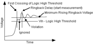
- verifying routed PCB layout: post-layout analysis consists of importing part or full PCB layout into a signal-integrity simulator. It is possible to determine with great accuracy the signals’ behavior in terms of the following: excessive distortion of the signal (ringing, excessive over/undershoots, non-monotonic edges, ringback etc.), excessive cross-talk, excessive losses (insertion and return) and excessive noise due to power integrity issues.
Below you can see three points which highlight the importance of Signal-Integrity analysis:
 1Developing a PCB board, with a signal-integrity approach in mind, mainly consists of identifying the most critical nets and defining for the first electrical (e.g. max. delay, max. overshoot) and then geometrical (e.g. min. distance, max. parallel length, trace topology) rules in order to satisfy the noise budget requirements. Connections between modern ICs, if not properly handled, tend to generate a hi-level of noise (mainly due to the signal’s reflections, cross-talks and SSO) which could be responsible for missing your signals’ timing requirements (e.g. non-monotonic edges, excessive ring-back voltage), premature component degeneration (e.g. repetitive excessive over/undershoot) and IC overheat (due to unwanted currents flowing into input clap diodes).
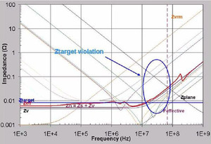
 2Hi-speed design also requires that particular attention is paid to the IC power supply (Power integrity analysis). This is another critical aspect which, in recent times, has become increasingly more significant due to the ever greater demands of IC voltage ripple requirements (e.g. max ±30mV on 1V@8A up to 200Mhz). Power Integrity analysis has the role of designing and/or verifying the PCB’s PDS (Power Delivery System). The PDS includes the VRM (Voltage Regulator Module), the bulk decoupling capacitors, vias, traces, planes and MLCC capacitors. Designing/Verifying the PDS means taking care of all of its components, in order for the PDS’s impedance profile to stay below a specific level (Z-target) up to a certain frequency (F-effective).

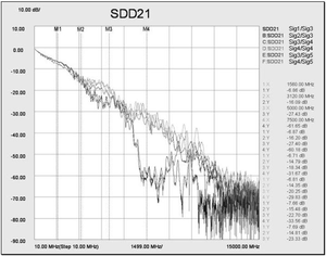
3Gigabit Serial-Links is another area where a signal integrity approach is highly recommended. Many Gigabit interconnects are built on top of the serdes function (e.g. Gigabit Ethernet, Serial RapidIO, PCI Express (PCIe)), as data transfers continue to increase, it is very important to be able to quickly and accurately evaluate and optimize the channel for performance through simulation. For example which connectors have acceptable performance? What impact do board structures like vias have? Which trace loss budgets are needed?
A Signal-Integrity approach to your projects will help your company to improve the overall quality of your products, giving:
- system stability in all working conditions
- fewer development risks
- no delays and/or extra-costs due to heavy project re-spin
- a better trade-off between PCB costs and board performance
- better EMC performance
If you require further information please do not hesitate to contact us.